Over the last 50 years photons, the particles that make up light, have replaced electrons to transfer data in communication networks. The very large bandwidth of optical signals has driven the enormous growth of telephone systems, television broadcasting and the internet.
However, photons have not yet replaced electrons in computers. Using light for transmitting data in processor chips and their interconnections would allow a substantial increase in the speed of computers (the speed of on-chip and chip-to-chip communication could be increased by a factor of 1000) and at the same time reduce the power required for them to operate.
Today’s most advanced microprocessor chips can contain tens of billions of transistors, and their copper electrical interconnections produce large amounts of heat when in operation. Unlike photons, electrons have a mass and an electrical charge. When flowing through metals or semiconductor material, they are scattered by the silicon and metal atoms, causing them to vibrate and produce heat. Therefore, most of the power supplied to a microprocessor is wasted.
The challenge of emitting light from silicon
Today the whole electronics industry is geared up to use silicon in computer chips because of the advantageous electronic properties of this material and its availability. It is a good semiconductor, a very abundant element and – as silicon oxide – a constituent of glass and sand.
However, silicon is not very good at dealing with light because of its crystalline structure. For example, it cannot generate photons or control their flux for data processing. Researchers have investigated light-emitting materials, such as gallium arsenide and indium phosphine, but their application in computers remains limited because they don’t integrate well with current silicon technology.
Shaping photonics chips: towards a revolution in the electronics industry
Recently, European researchers reported in the journal Nature an innovative alloy of silicon and germanium that is optically active. It is a first step, says Jos Haverkort, a physicist at the Eindhoven University of Technology in the Netherlands: “We showed that this material is very suitable for light emission, and that it is compatible with silicon.”
The next step is to develop a silicon-compatible laser that will be integrated into the electronic circuitry and be the light source of the photonics chips. This is the ultimate aim of the project SiLAS, supported by the EU programme FET. The team, led by Erik Bakkers from the Eindhoven University, also includes researchers from the universities of Jena and Munich in Germany, Linz in Austria, Oxford in the UK and from IBM in Switzerland.
To create the laser, the scientists combined silicon and germanium in a hexagonal structure, which is able to emit light, overcoming the all known uses of silicon where the atoms are arranged in a pattern of cubes. And it has not been easy. An initial attempt to coax silicon into adopting a hexagonal structure by depositing silicon atoms on a layer of hexagonal germanium failed.

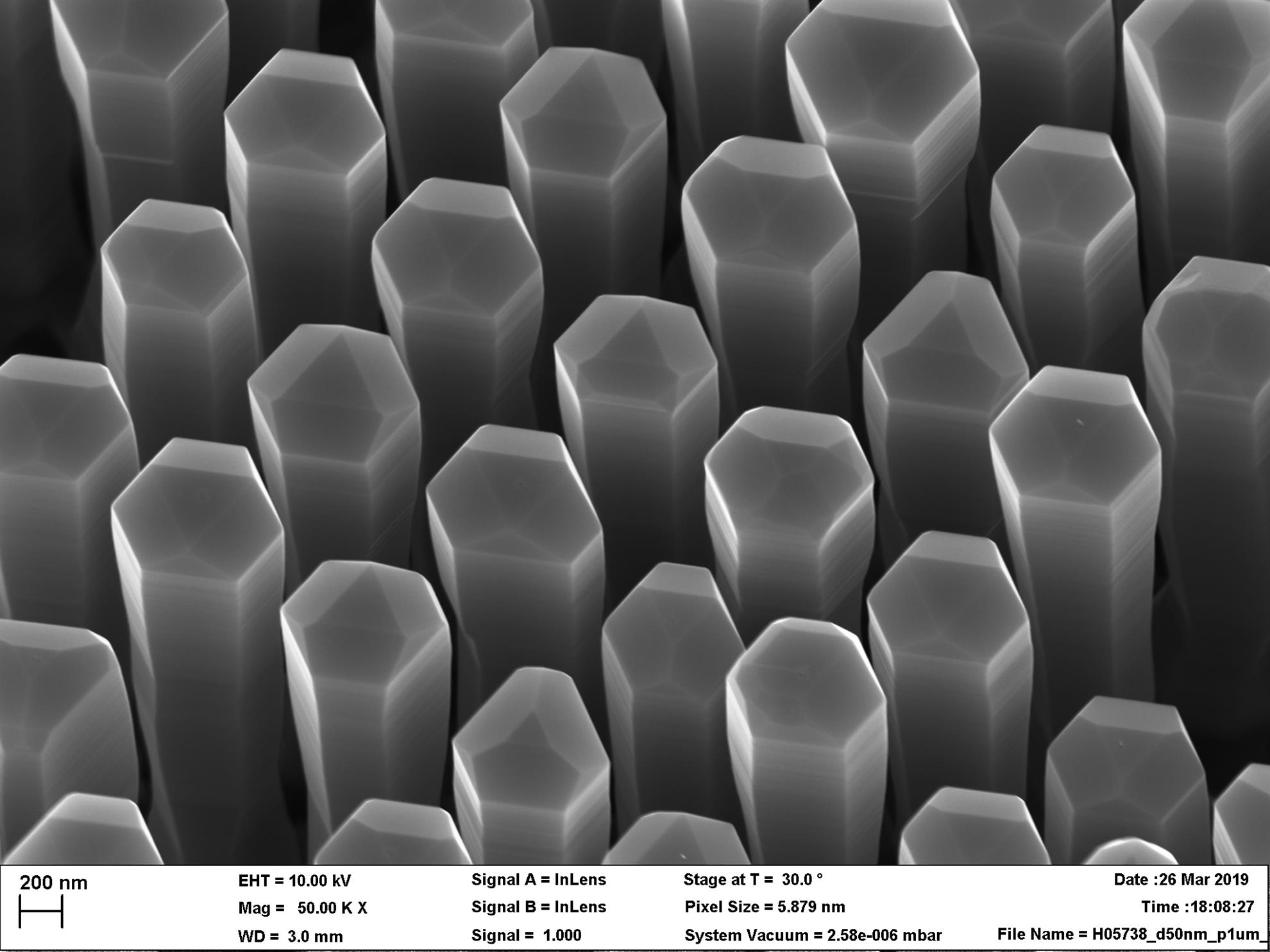
Nanofibers of germanium-silicon alloy with a hexagonal crystalline structure, which can emit light and are compatible with current silicon semiconductor technology. Credits: Elham Fadaly, Eindhoven University of Technology
Silicon stubbornly refuses to change its cubic structure when grown on planar hexagonal germanium, explains Jonathan Finley of the Technical University of Munich, and who took part in the research by measuring the optical properties of the created silicon samples. “You have to convince Mother Nature to allow the growth of this unusual form of silicon germanium. It likes to grow cubic, that is what it does,” he says.
However, over the years the research group at Eindhoven has developed expertise in growing nanotubes, and reasoned that what does not work on a planar surface of germanium might work on a curved surface of a nanotube. And this time things worked out. "What we did was to use a nanowire of gallium arsenide, which has a hexagonal structure. So we had a hexagonal stem, and we created a silicon shell around the core, which also had a hexagonal structure," says Haverkort.
By varying the amount of silicon and germanium deposited on the nanotubes, the researchers found that the hexagonal alloy was capable of emitting light when the concentration of germanium was above 65 percent.
Now, the proof of the pudding would be a demonstration of lasing, in other words how the silicon-germanium alloy can amplify and emit light as a laser, and measure it.
There are several open questions to resolve before silicon germanium can become fully integrated with silicon-based electronics, remarks Haverkort: “First, these devices have to be integrated with existing technologies and that is still a hurdle.” He expects that future quantum computers will use applications such as low-cost silicon-based LEDs, optical fibre lasers, light sensors, and light-emitting quantum dots.
In general, the shift from electrical to optical communication will boost innovation in many sectors, from laser-based radars for autonomous driving to sensors for medical diagnosis or air pollution detection in real-time.
youris.com provides its content to all media free of charge. We would appreciate if you could acknowledge youris.com as the source of the content.